A real-time clock addon for Calculon/80
A real-time clock addon for Calculon/80
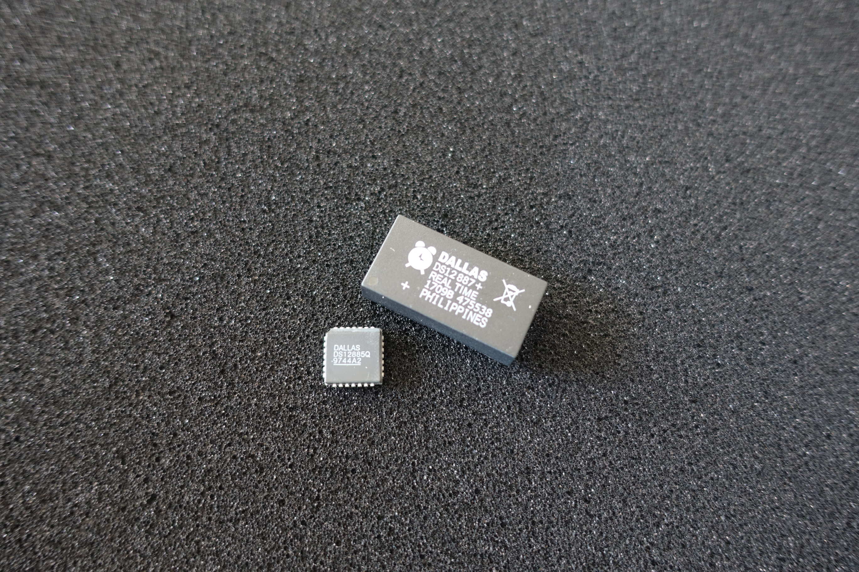
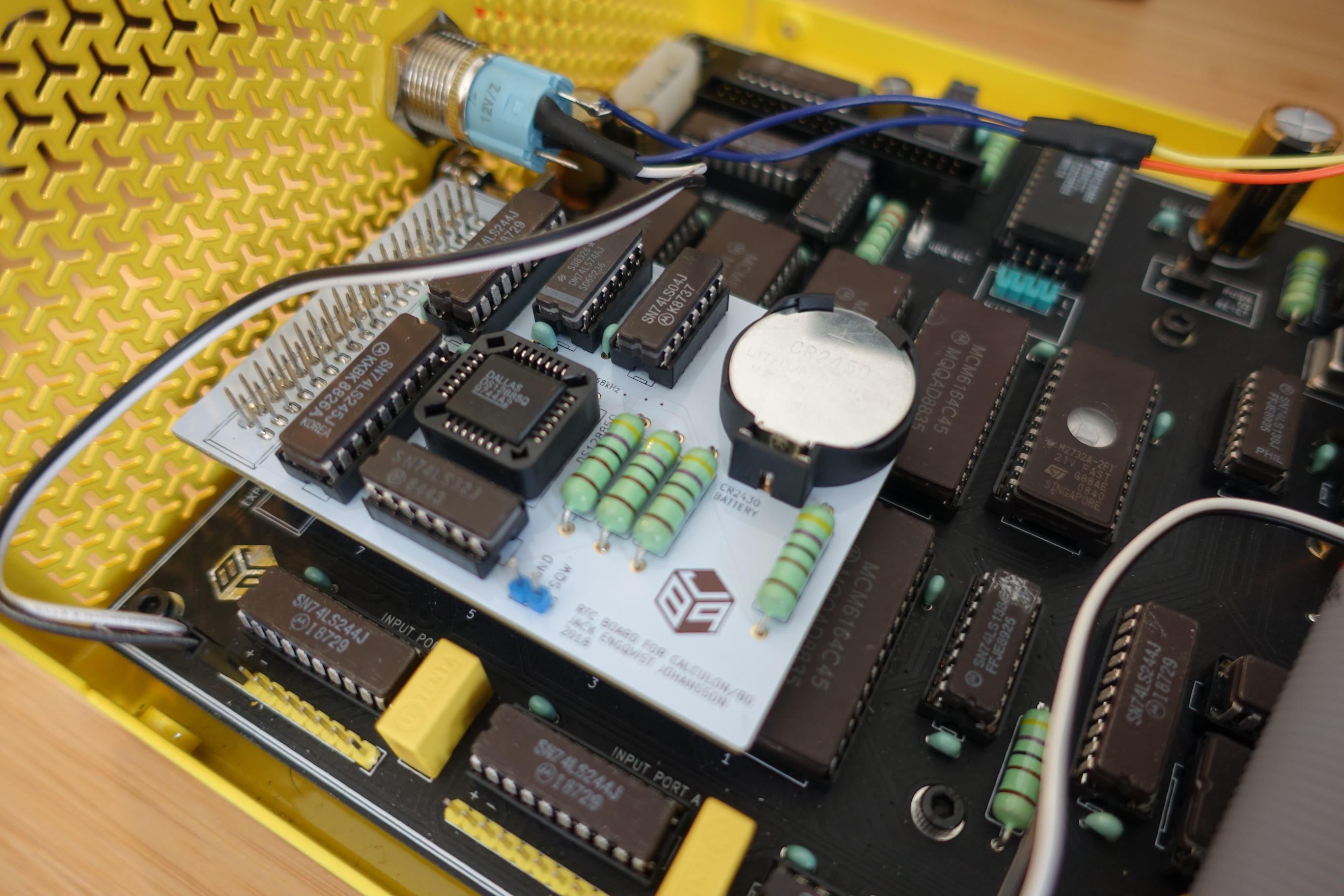
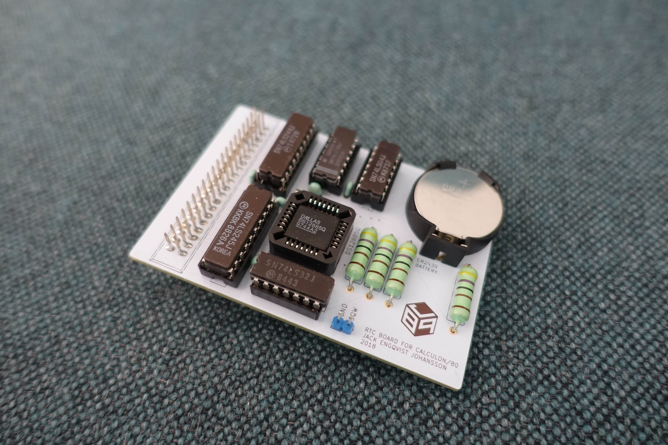
I wanted the Calculon/80 to have a real-time clock and some battery backed RAM for storing BIOS settings so I decided to use the Dallas DS12887 RTC with built-in lithium battery. It keeps track of time and date even when the computer is unplugged from the power supply. There are other alternatives available but it is the one used in the IBM AT computer, which makes it the right kind of retro that I want in the Calculon/80. An easier solution would be to use the BQ4845, which is a lot simpler to interface with the Z80, but it felt more like a something for embedded systems with features like watchdog timer etc.
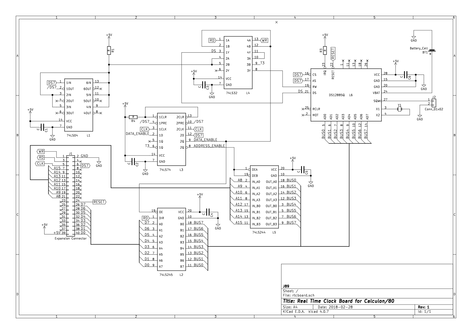
Multiplexed data and address bus
One problem with the DS12887 is that is has a multiplexed address and data
bus, which means that the data bus and address bus share the same pins but
the data are latched at different times. The buses on the Z80 are not
multiplexed so I had to think out a solution. My first idea was to simply
write to it as it was two IO devices, one for latching the address lines
and another one for the data. I didn’t try this, but according to the
datasheet, it shouldn’t work due to the CS (Chip Select) line, which
cannot be de-asserted without losing the latched address. So I must write or
read to it during a single IO cycle, luckily, the IOREQ line on the Z80 is
lowered a T-cycle before the RD and WR lines. I could therefore use this to
latch the address by connecting the IOREQ to AS (Address Strobe).
The buses can be demultiplexed by using two three-state bus buffers, a
bidirectional for the data bus and a unidirectional for the address bus.
The direction of the bidirectional buffer is controlled by the RD line on
the Z80. The address buffer should be in three-state mode after the first
T-cycle, and vice versa for the data buffer. I used a D-type flip-flop to
delay the DS7 signal and then connected that to the data buffer’s
output enable pin. The inverted signal where connected to the address
buffer’s output enable pin.
Control bus
Now when the address and data buses are demultiplexed, I only need to make sure that the DS12887’s control lines are asserted at the correct times. The CS pin where connected directly to DS7 signal to latch in the address. I also connected the CS pin to DS7, which is OK since the address can be latched without the CS pin is being asserted.
The R/W (Read/Write, Write-Enable in my case) and DS (Data Strobe) pins are not that easy.
Data Strobe
The DS pin should be asserted when it is safe for the RTC to drive the bus, i.e. it acts like OE (Output-Enable) on memory ICs. The DS line should only be asserted (lowered) during the data part of a read cycle, which means that both the RD line and the new DATA_ENABLE line should both be 0. I used a 74LS32 (OR gate) for that, and connected the output to the DS pin.
R/W
The R/W pin latches the data on the rising edge of the signal, which should only be done when the CPU has driven the bus with data for atleast 100 ns. The signal could be generated the same way as with the DS signal, but using the WR instead of the RD signal. But this will assert the R/W signal on the same time the data is placed on the bus (plus the propagation delay for the OR gate). Since the signal needs to be delayed atleast 100 ns as well as being inverted (because it is positive edge triggered), I had to use a D-type flip-flop to create a delayed DATA_ENABLE signal. The complementary output (i.e. the delayed and inverted DATA_ENABLE signal) were connected to another OR gate which output were connected to the R/W pin.
Conclusion
When designing the PCB I decided to replace the DS12887 with a DS12885. They are essentially the same but with the difference that the DS12887 has built-in battery and crystal. For me, that’s a drawback since the entire IC needs to be replaced when the battery runs out.