Worklog
Content
Introduction
This is the worklog for the first few milestones of building the computer; getting it to work on breadboards and then designing a PCB using KiCAD. Things that comes after, such as enclosure and software, will be documented as blog posts instead.
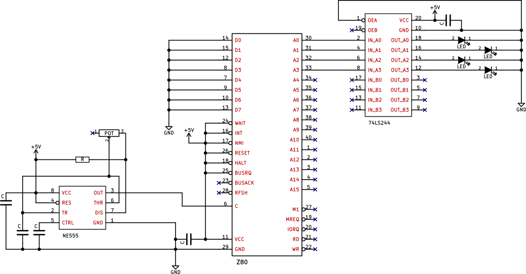
Wiring up the Z-80
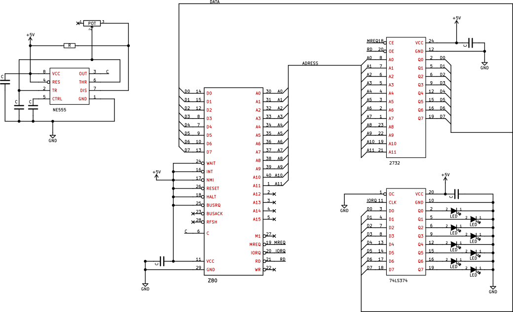
To quickly test that the Z-80 and clock was working, I wired up a
minimal circuit with a clock, a Z-80 and some LEDs. It is not
capable of doing something useful but it is an easy way to get started.
The data lines are connected to ground to simulate a NOP instruction to
allow the PC register to increase. I used some LEDs and a 74LS244 bus
driver connected to the address bus to make it visible.
As a clock, I used an NE555 to generate a clock signal which can be
changed using a potentiometer. The Z-80 now runs at a speed at around
1 Hz which makes it really simple to follow the address bus counting.
Decoupling capacitors are placed near the Z-80 and ‘LS244 as possible to make sure that the system is running stable. This will also be done for all ICs added to the computer in the future.
Connect ROM and I/O
Now that I know that the microprocessor, along with the clock and power supply is functional, it is time for something more fun. I added ROM and a parallel output port to let the Z-80 execute a program that blinks some LEDs. Four LEDs connected to a 74LS374 (octal latch) was used as an I/O port. No address decoding are done at the moment so this is the only device addressable so far. The ‘LS374 samples the data lines on the rising edge of the CLK pin. This is connected to the /IORQ pin on the Z-80 which goes high the T-cycle before the data lines changes. To keep the state even after /IORQ goes high, the /Output-Control pin on the ‘LS374 is connected to ground.
EPROM
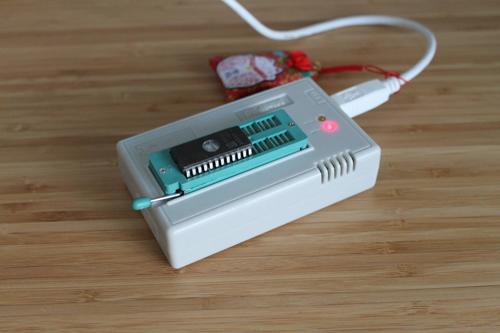
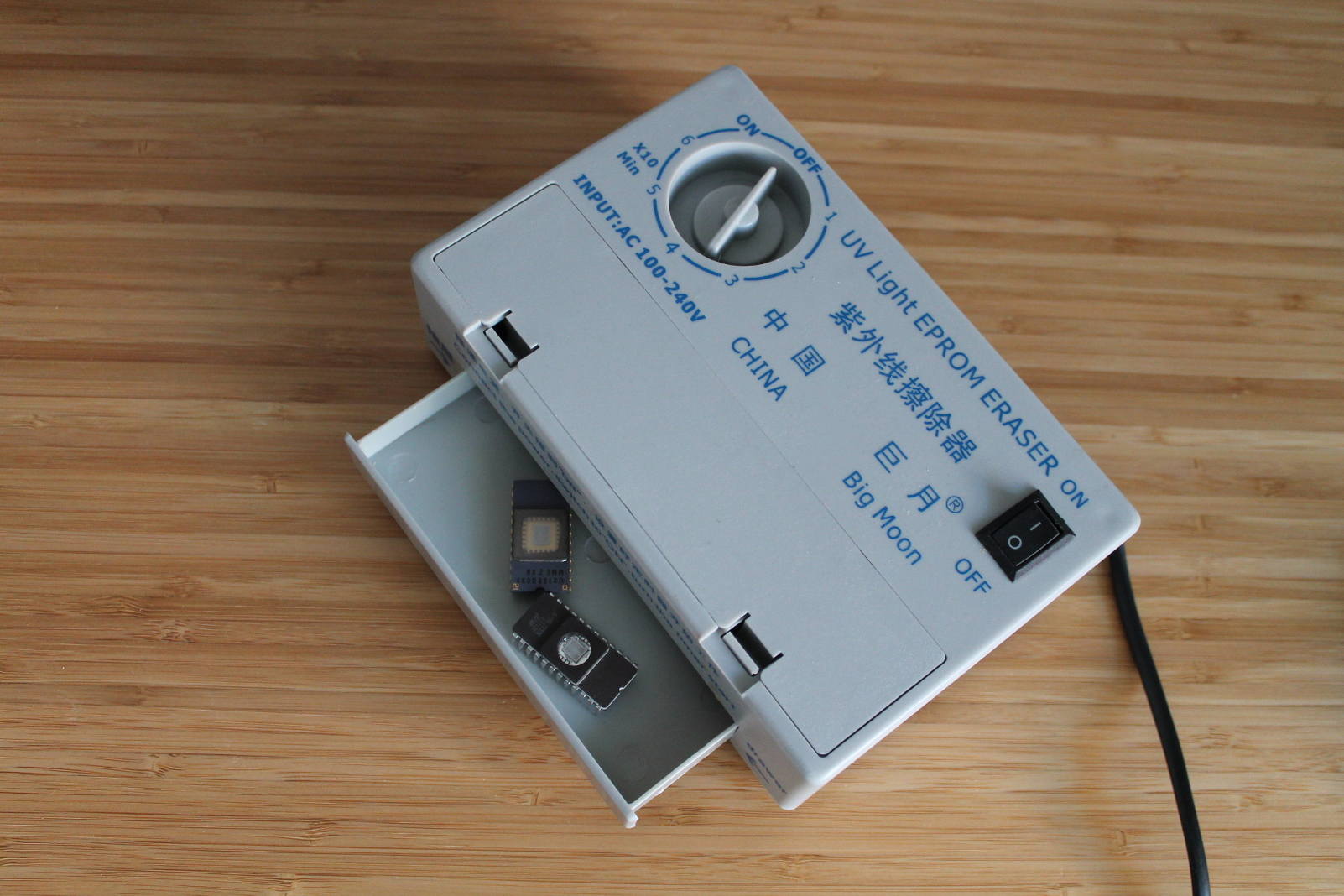
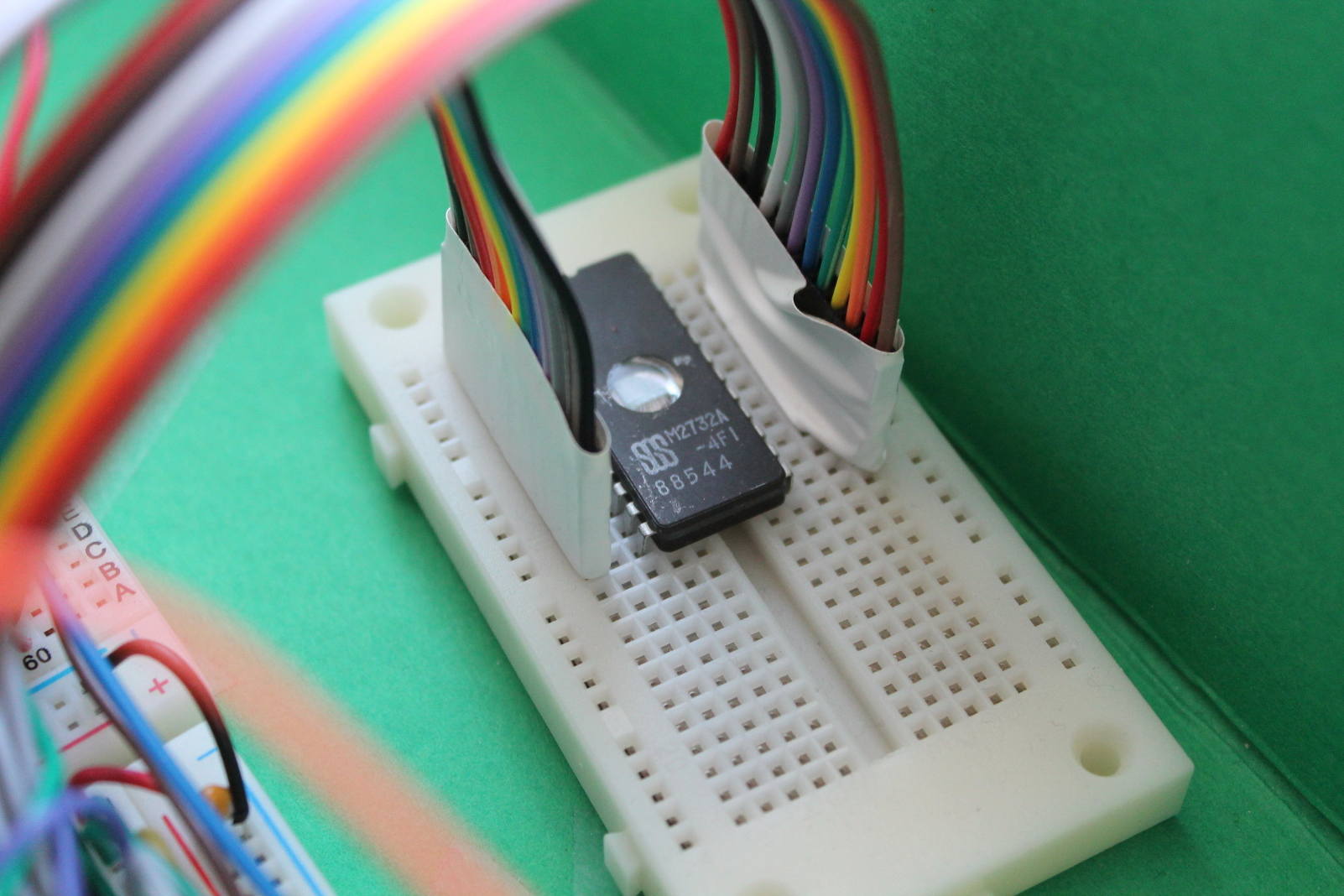
The ROM I picked was a 2732A UV EPROM (4 KiB). To store a test program
on it I needed an EPROM burner. While it had the ‘A’
suffix, it only needs 21V programming voltage in contrast to the regular
2732 which needs 25V. I bought a universal USB programmer from eBay
called ‘TL866CS’, which can program EPROMS with voltages up
to 21V without any other power source than USB.
The /Chip-Enable and /Output-Enable pins on the EPROM are connected to
the /MREQ and /RD pins on the Z-80. This enables the EPROM only when a
read from memory is desired.
The Program
The test program switches between the output values 00000000B and 11111111B without any other delay than the time it takes to execute the instructions.
        ORG

	MAIN    XOR     A
	        OUT     (00H),A
	        LD      A,FFH
	        OUT     (00H),A
	        JP      MAIN

	        END
Schematic
Only 12 of the address lines are connected because the ROM has 4096 (2^12) locations.
Connect RAM
Now it’s time to add some RAM to the computer. I could pick a 64 KiB big read-write RAM, like the 62512, to fill up the entire address space without the need for any decoding. However, I have alot of ceramic 6164 SRAMs that I want to use instead. They are 8 KiB each so eight of them are needed to fill the address space. Splitting up the address space also makes it more simple to switch in and out ROM (next chapter). For the address decoding I used a 74LS138, which is a 3-line to 8-line decoder and is perfect for this use case. The three highest address lines A13, A14 and A15 where connected to the three binary inputs on the ‘LS138. One of the eight active-low outputs will be active at a time depending on those three lines. Each RAM ICs Chip Enable pin is connected to one output line. The Chip Select pin on the ‘LS138 is connected to /MREQ on the Z-80. When /MREQ goes high, all the output lines goes high, which disabled the RAM ICs. The /RD and /WR lines are connected directly to the respectively pins on the RAM and EPROM.
Switch out ROM
The computer should be able to run CP/M which requires page zero to be
RAM, but page zero is occupied for the moment by ROM. This is due to
the fact that the Z-80 starts to read instruction from address 0x0000
so it can not be occupied by RAM on boot. The solution to this is to
copy the ROM code to RAM, jump to the new location and then switch out
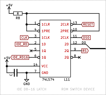
the ROM to RAM. As a bank switching device, I used a 74LS74, a D-type
edge triggered flip-flop. The output Q of the ‘LS74 is connected
to both the /Chip Enable pin on the EPROM and the /Chip Select on the
page zero RAM. The 6164 RAM has two chip select pins, one active-low
and one active-high. While the /Chip Enable pin on the EPROM is
active-low, the active-high pin on the RAM can be connected to the same
output on the ‘LS74 as the EPROM.
The ROM has to be selected by default when the computer is reset. I
solved this by connecting the /CLR input on the ‘LS74 to the
/RESET. When /CLR, which is acive-low, goes low, it resets the
‘LS74 output Q to logic 0.
As the ‘LS74 is an additional IO device, the IO address space of the Z-80 must be decoded to allow multiple devices. I used the same logic as in the memory address space decoding, a ‘LS138. This allows me to have a total of 8 addressable devices without any additional logic. I connected the address lines A3, A4 and A5 to the ‘LS138. This means that each addressable device occupies 8 locations (0x00..0x07, 0x08..0x0F, 0x10..0x17, etc.).
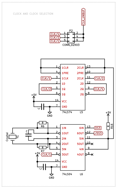
Faster clock
It is time to get rid of the N555 circuit and add a faster and more stable clock. There is several ways to build an oscillator but I wanted to use a crystal and 7400 series ICs, so I went with the series resonant oscillator circuit. It is a simple oscillator that only requires a crystal and a couple of inverters, like the 74LS04. The output is a square wave clock signal in the same frequency as the crystal. It is important that the signal is clean enough for the Z-80 which requires a maximum of 0.45 V as low and 4.75 V as high (4.40 V for CMOS). The output looks like this:
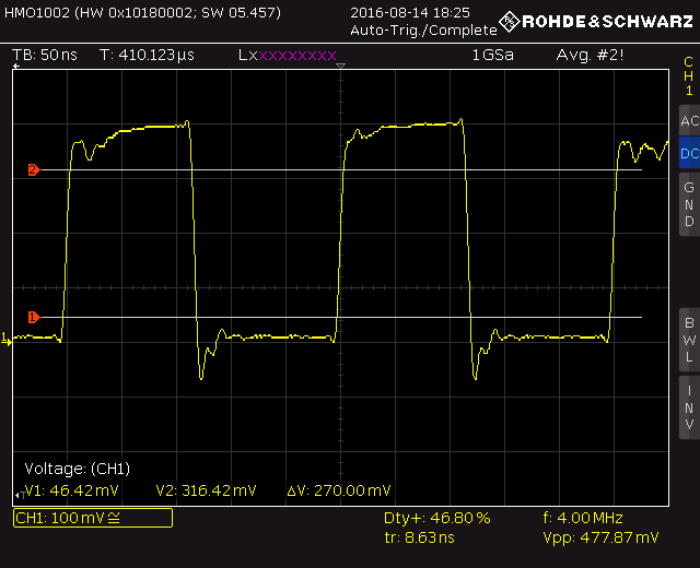
The amplitude just reaches 3.4 V, this is because the typical output voltage for a 74LS04 is 3.4 V. However, it does work for some reason.
I wanted the possibility to choose between different frequencies so I added a 74LS74 as a frequency divider. It contains two flip-flops so the frequency can be divided by 2, twice. If i have a 4 MHz crystal, I get the following frequencies; 4 MHz, 2 MHz and 1 MHz. All the frequencies are selectable via a double row pin list and a jumper. As an alternative, it could instead be possible to use a data multiplexer, like the 74LS151, to select a frequency dynamically.
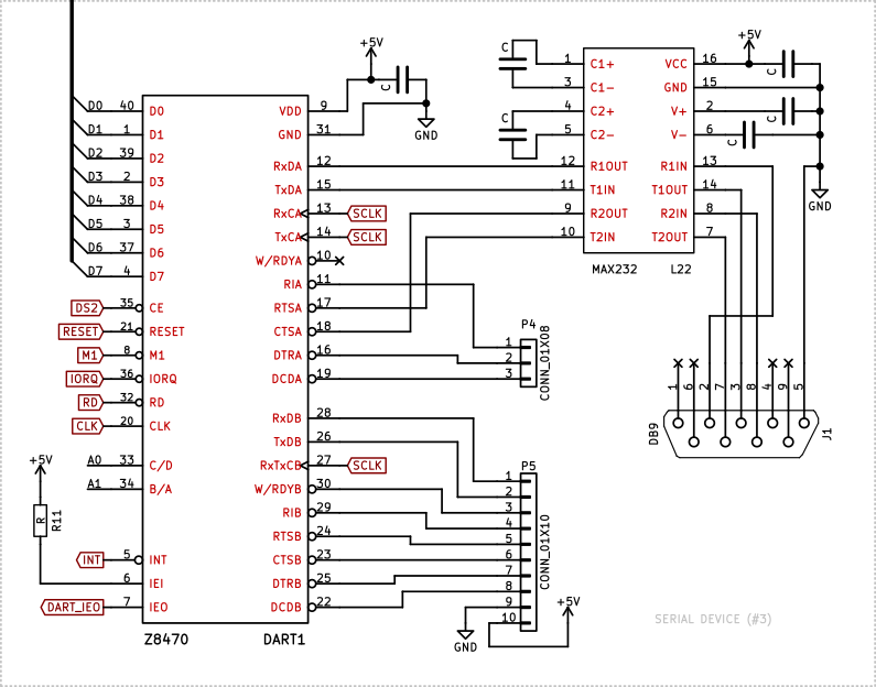
Installing serial interface (DART or SIO)
The Z8470 (Z80DART, Dual Asynchronous Receiver Transmitter) is used as a serial interface. It is connected to the I/O address space by the /Chip Select that is connected to the ‘LS138. The Control/Data pin is connected directy to A2 on the Z-80, which makes both the control registers and data register easely accessible at separate addresses. The DART's data register is placed on address 0x10 and the control registers on 0x11. To allow addressing both channels, the A/B pin is connected to the address bus in a similar way as the Control/Data pin.
Bus buffering
The Z-80 only supports one TTL load per line and the number of connected ICs starts to add up, so it's time to buffer the Z-80 buses. Because the address bus is unidirectional, a simple line driver can be used, like the 74LS244. Two of them are required, because the address bus is 16-bit wide and the 'LS244 is 8. The data bus is different, it is bidirectional and a 'LS244 can not be used here. Instead a single 'LS245 will do the job. The 'LS245 is an octal bus transceiver and can buffer the lines in both directions. The direction is controlled by the DIR input, which I connected to the /RD pin on the Z-80.
Propagation Delays and Timing
When adding glue logic like this, it is important to verify that the timing is still functional. Here is a table of the maximum propagation delays of the logic ICs:
IC              P-delay (nS)    Enable-delay (nS)
	74LS245         12              40
	74LS244         18              30
	74LS138         18              32
	74LS374         28              28
This is the worst case delays and is typically much lower. Lets have a look at the timing in the opcode fetch cycle, M1. The address is set at the rising edge of the first T cycle while the /RD and /MREQ lines are set at the falling edge of the same T cycle. The opcode is clocked in from the data bus at the rising edge of the third T cycle. This means that the glue logic and memory have one and a half T cycle to respond. At 4 MHz, a T cycle is 250 nS, so one and a half T cycle is 375 nS. The EPROM I used, M2732, has an access time of 200 nS. This leaves 125 nS for the glue logic. The address bus, that is buffered by an ‘LS244 with a propagation delay of 30 nS, will still be set before the falling edge of the first T cycle. So the potential problem may lay in the address decoding, which relies on the /RD and /MREQ lines. The ‘LS138 used as address decoder has a propagation delay of 32 nS. But the /RD line is buffered with an ‘LS244, which adds an extra 18 nS. The reason it is only 18 nS is that the ‘LS244 is always enabled. The total delay for the address decoding adds up to 50 nS. When the output data at the EPROM is valid, it is buffered by an ‘LS245 that adds 12 nS before it can be clocked in by the Z-80. Adding all the delays together results in 262 nS, and this is the absolute maximum and is probably much lower in reality.
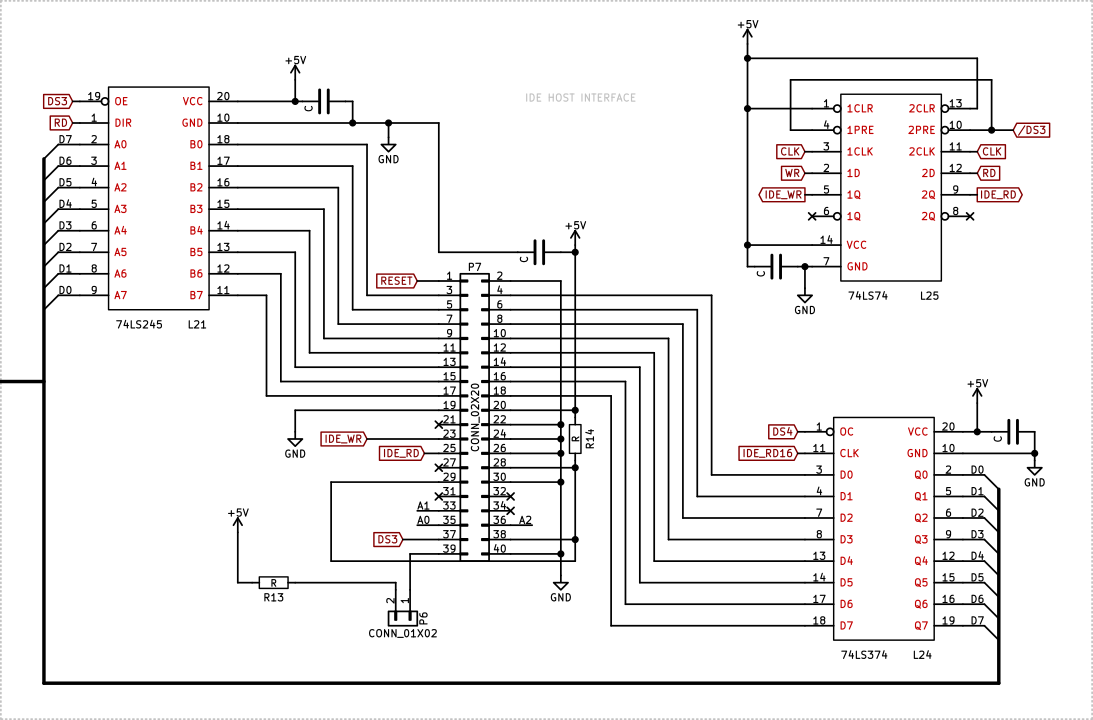
Designing an IDE host interface
The IDE interface is quite easy to implement and is widely used, and that’s the reason I went with it, instead of a floppy disk controller. The buses are parallel and easy to connect to the Z-80. The only problem is that the databus is 16-bit wide while the Z-80’s is only 8. Actually, the control registers are 8-bit, it is only the data register that uses the full width of the data bus. It is possible to leave the higher 8 bit and only use 8 bits, but then only the half of the disks storage can be used. This is a common thing to do with homebrew computers but the simplicity comes with another drawback; it is not possible to read the entire disk parameter data structure. To half the disks capacity is okay for me, but I want to be able to read the disks parameters, like the ID etc. This was my requirements when designing the IDE host interface. My final design is able to read 16-bit but only write 8-bit, which is lets me read the entire disk parameters but only use half of the disk space. It is a really simple design but still very functional.
A good place to start is to read the specification. I went with ATA-2
(EIDE) specification because it is much simpler than the newer ones.
It is straight forward to connect the lower 8-bit of the data bus and
the two address lines along with the /CS pin. After a quick look at
Wikipedia I learned how to connect the remaining pins, like ground and
activity etc. The tricky part is the timing, which is not compatible
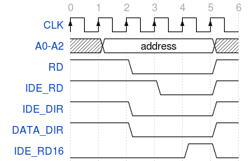
with my current design. The first lines to become stable in a read
cycle is the address lines followed by /RD and /IORQ in the second
T cycle, like I described earlier. The /CS relies on the address lines
and /IORQ and will therefore be 18 nS behind /RD. The ATA-2
specification requires that the address lines along with the chip select
lines are stable a minimum 70 nS before the /IORD or /IOWR pins goes low.
This is not the case for me where the /CS is the last pin to get active.
My solution to this was to use clocked logic using an ‘LS74
flip-flop, to delay the /RD and /WR signals to the rising edge of the
next T cycle, which should be more than 200 nS later. The ‘LS74
has two flip-flops, one is used for /RD and the other for /WR. The CLK
pins are connected to the system clock and the data pins to the buffered
/RD and /WR pins from the Z-80. The output are connected directly to the
IDE interface pins /IOWR and /IORD. They will only be active when the /RD
and /WR are active at the rising edge of the clock, which is the third
T cycle. To make sure that the output is only active during a read or
write cycle related to the IDE interface, I connected an inverted /CS
line to the /PRESET pins on the flip-flop. When the IDE is not selected,
the IORD and IOWR will always be high.
The /IORD or /IOWR lines must me stable at least 165 nS before any read or write occurs. In case of a write, the data bus will be stable in the middle of the first T cycle and will be stable for more than three T cycles ahead, which is 250 nS each, so that’s fine. The read cycle is a bit more complicated. The 8 lowest data bits will be clocked in by the Z-80 in the fourth T cycle, which is approx 500 nS later, but the problem is the higher 8 bits. They need to be latched at the right moment and then be read afterwards. I used a third ‘LS74 flip-flop to delay the /IORD signal an extra T cycle and connected it to the CLK of an ‘LS374. Actually, I used the complementary output (/Q) of the ‘LS74 because the ‘LS374 samples the data at the rising edge of the CLK input. The data inputs of the ‘LS374 where connected to the higher 8 bits.
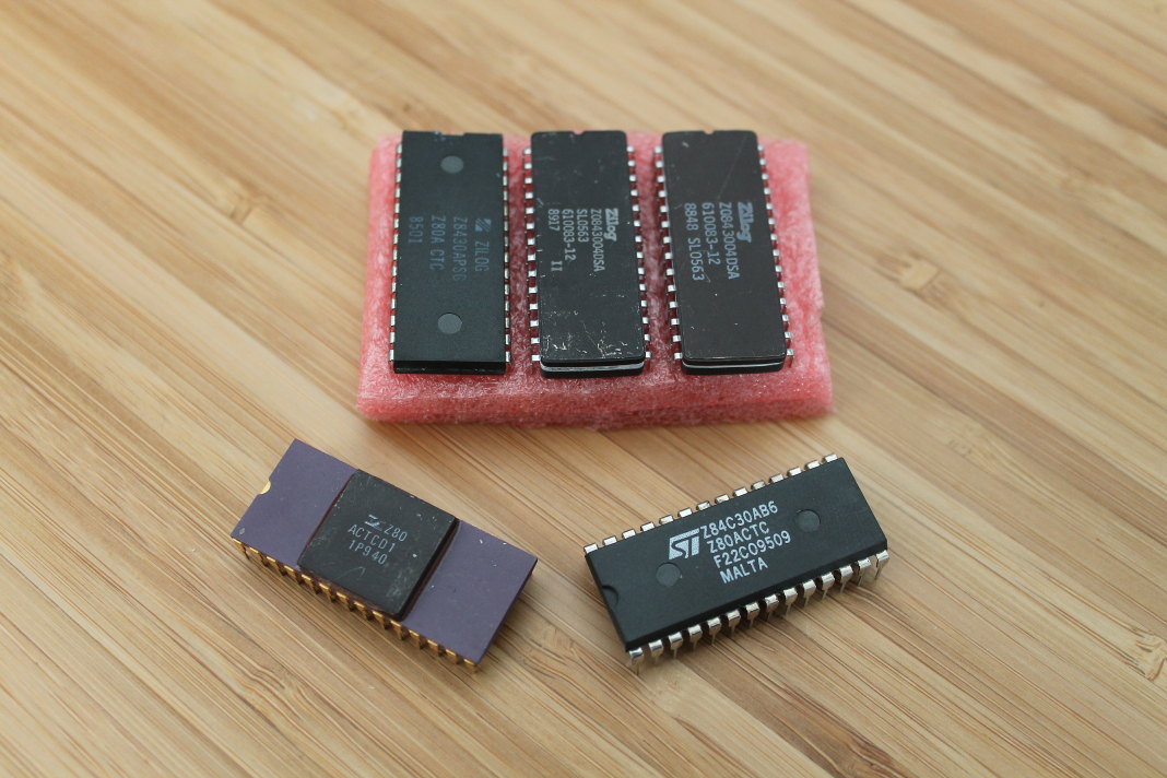
Installing timer (Z80CTC)
I want the computer to have some kind of timer which can be used to keep track of time or to be programmed to interrupt the Z-80 periodically or after a specific delay. I found the Z-80 peripheral timer IC Z8430 (Z80CTC) the easiest way to do this. Because it is designed for the Z-80 it is straight forward to use. However, this was the first component to utilize the /INT line, which is a bit different from the others used so far because it is an open-collector input. I added a pull-up resistor to the /INT line and then connected it to the /INT in the CTC.
While the CTC handles all the interrupt logic for itself, I got a problem with the device address decoding in case of an interrupt. The /IORQ line, which is used in the device address decoding, is also used, along with M1 to acknowledge an interrupt. In my case, this would cause problems because the interrupting device should get access to the data bus, not the accidentally addressed device. To fix this, I had to connect the /M1 line to E3 on the ‘LS138. The E3 is an active-high enable pin, which makes the device address decoding enabled only if /IORQ is low and /M1 is high, which is not the case of an interrupt acknowledgment cycle.
There was also another issue that had to be solved, the direction of the data bus buffer can no longer be controlled by the /RD line alone, because it doesn’t get low during an interrupt acknowledgement cycle. The bus buffer need to be in read mode during an interrupt acknowledge cycle because the interrupt vector is placed on the bus at that time. The direction will instead be determined in the following way; (/M1 ∨ /ÌORQ) ∧ /RD. It may be confusing, because the lines are active-low. To clarify it a bit; the new line DIR should be low only when /RD is low or when both /M1 and /IORQ are low. Due to the fact that all lines are active-low, a regular AND gate can be used as an OR gate for inverted inputs and output. In the same way, AND gates can become OR gates.
The timer channel inputs and outputs where connected to a pin header. I shifted the inputs one step to make it possible to use a jumper to chain two channels together to make it 32-bits wide instead of 16.
More I/O devices
Up until now, the computer only have had one output port and no input ports at all. To add more GPIO, I could use a Z-80 PIO or simply add more ports in the same manner as earlier. I did not have a Z-80 PIO and adding more bus buffers and latches as I/O devices would only fill up the remaining chip select lines on the address decoding ‘LS138. I decided to use the same address space used for the current output port but divide it into another 8 chip select lines. For this, I used a 74LS155 to decode A0 to A2 into 8 new chip selects to be used as GPIO ports. I only used 4 of them, 2 ‘LS244 buffers for outputs and 2 ‘LS374 latches for inputs.
Reset circuitry
So far the /RESET line is just connected to Vcc through a resistor and to a push button which goes to ground. This works fine in cases where a running system needs to be reset, but can cause problems when the computer is first switched on because some components takes longer time to stabilize than other, for example the HDD. The solution to this is to simply delay the reset signal by adding a large capacitor between /RESET and ground and increasing the resistance of the pull-up resistor. When someone pushes the switch button, the capacitor will be discharged and the /RESET line will get active. After releasing the button, the capacitor starts to recharge through the pull-up resistor.
After I received the PCBs and started to test the computer I realized that the components may have different logic levels on the reset line. It could be various manufacturing technologies like CMOS and TTL but also other variations. A better solution would be to have two separate reset lines with different delays. One for the CPU and one for the rest. The CPU reset line should have the longest delay so when the CPU starts executing code the programmer can be sure that everything has been brought out of reset. The cheap fix I have to use now is to add a delay in software.
Fan-out calculations
Fan-out calculations will be published here as soon as they are done.
What could be improved
- 16-bit IDE Interface.
- IDE DASP Connected to 10K Ohm pull-down resistor.
- Utilize IDE interrupts.
- Optimize the use of device address space.
- Add a bus buffer to split the load.
- 10 uF capacitors at important ICs.
- Dedicated reset lines and capacitors, one for CPU and one for the rest. CPU should be last.
Ideas for a successor
- Bigger and fewer memory ICs.
- Banked memory.
- ISA bus or similar.
- Not single-board.
- Graphics and keyboard interface.
- Based on Motorola 68000.
- Use a 74LS151 to select clock source in software.
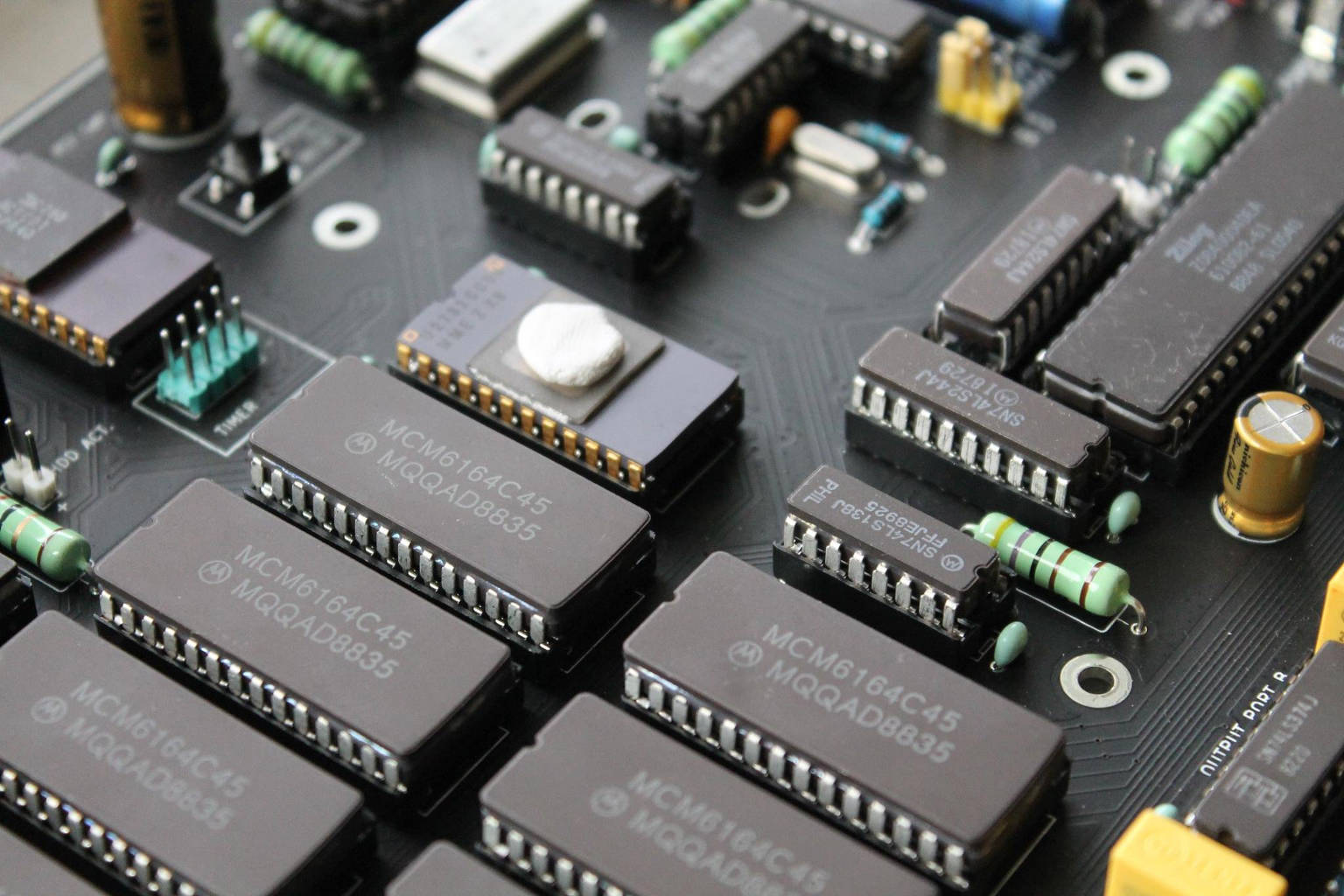
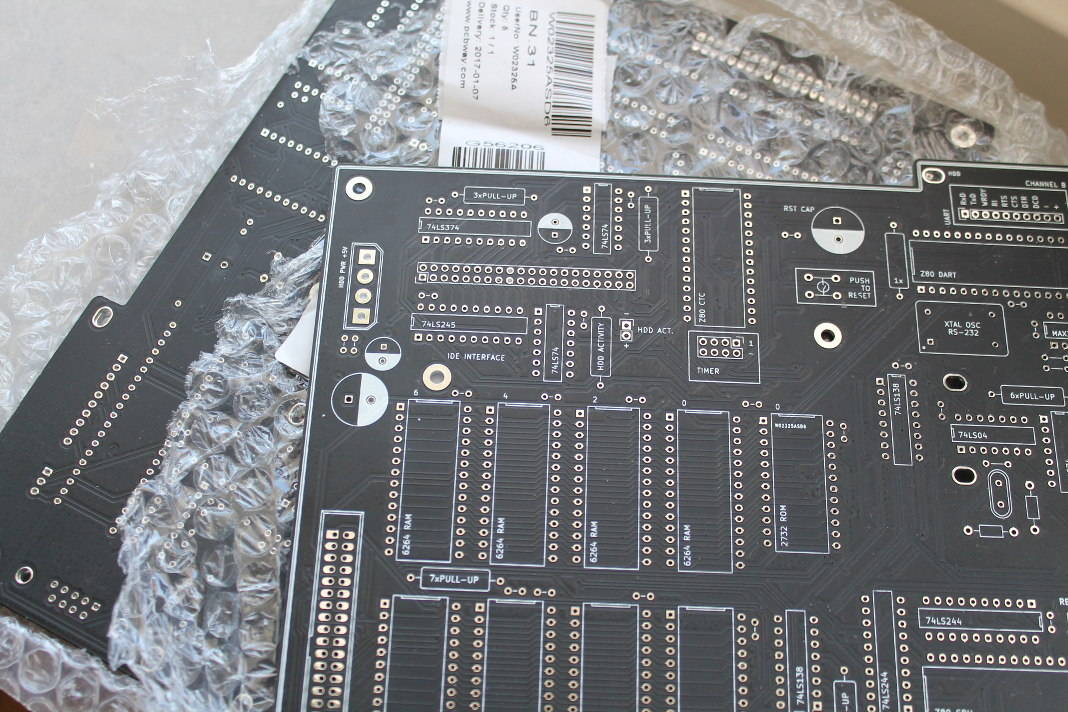
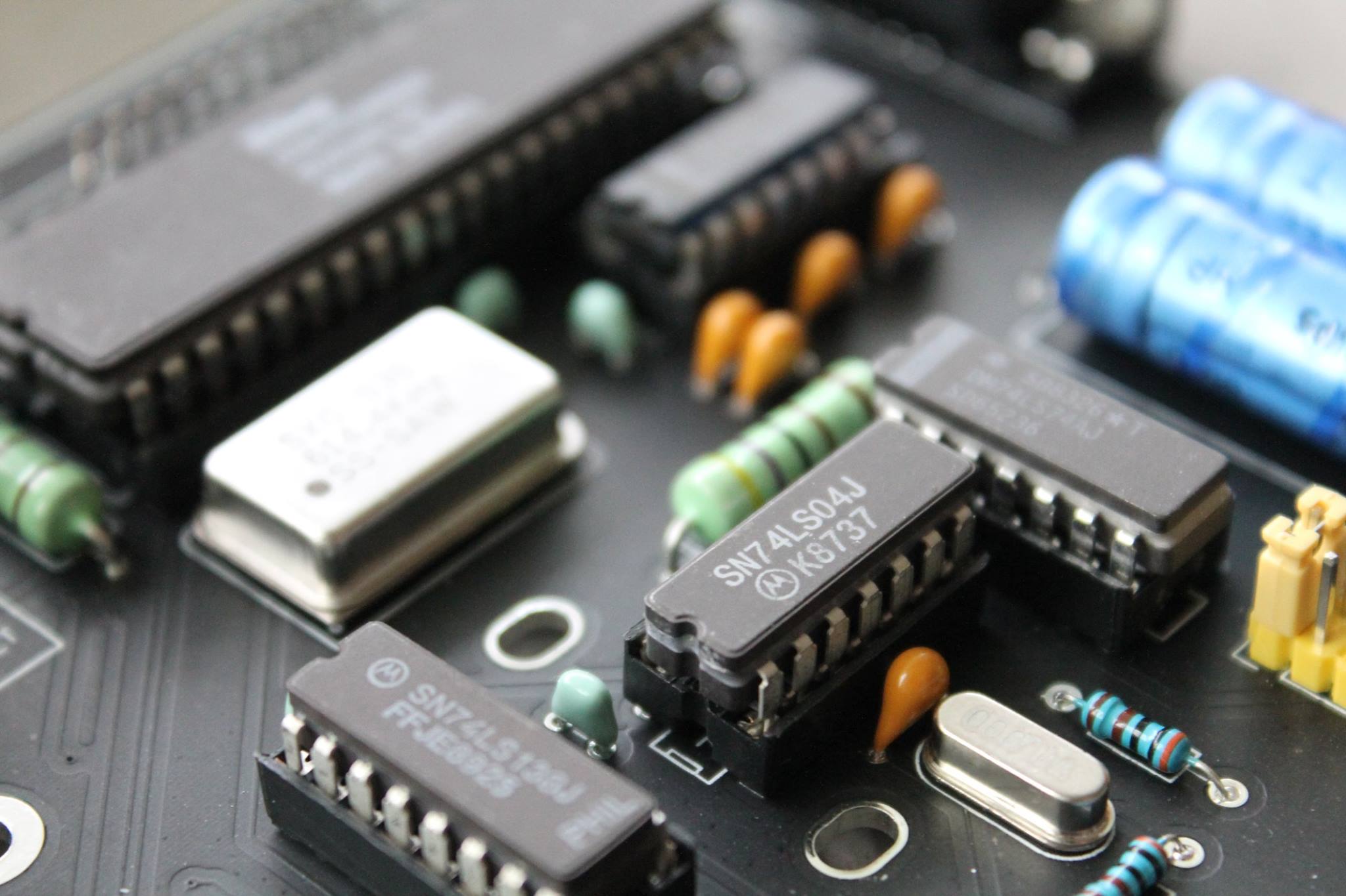
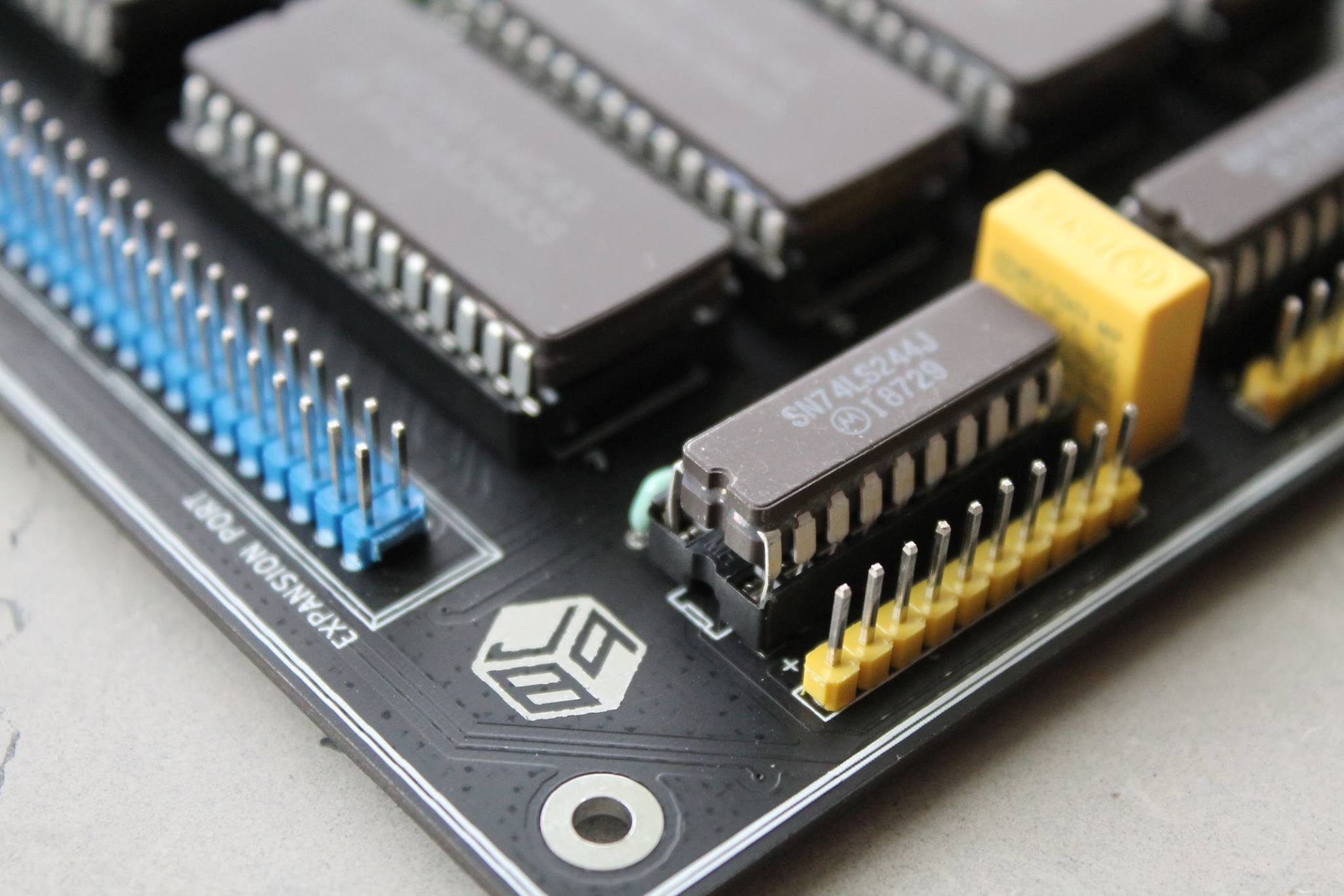
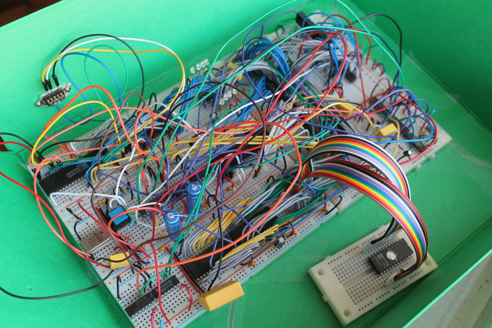
Photos